


Shining a light on electrons’ role in energy transfer among 2D materials
Simulations run at NERSC yield surprising findings
March 6, 2023
By Patrick Riley
Contact: cscomms@lbl.gov
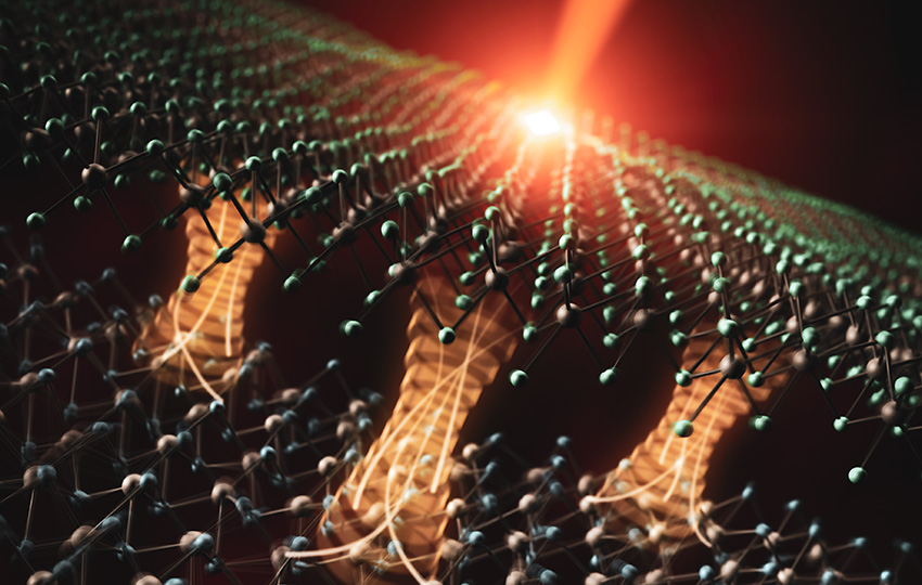
Artistic depiction of electron transfer driven by an ultrashort laser pulse, across an interface between two atomically-thin materials. This transfer is facilitated by an interlayer 'bridge' state that electrons are able to access due to lattice vibrations in both materials. (Credit: Gregory M. Stewart/SLAC)
Backed by supercomputing prowess at the National Energy Research Scientific Computing Center (NERSC) at Lawrence Berkeley National Laboratory (Berkeley Lab), a group of scientists examined heat and energy movements between certain two-dimensional (2D) materials, spurring discoveries that could pave the way for a new generation of transistors.
Marrying theory and praxis, the researchers shined a light on the surprising role electrons play in the energy transfer between layers of tungsten diselenide (WSe₂) and tungsten disulfide (WS₂), a pair of 2D semiconductor materials. In their study the scientists found that even though the layers aren’t tightly bound to each other, electrons provide a connection between them that dramatically speeds up heat transfer.
This class of atomically thin materials could lead to advances in new electronic devices, but one of the challenges with those materials has been that the heat dissipation is “very slow, to the point of being a bottleneck for many practical devices,” said Felipe da Jornada, an assistant professor of materials science and engineering at Stanford University, a principal investigator at the SLAC National Accelerator Laboratory, and a co-author of the paper, which was recently published in Nature Nanotechnology.
However, the researchers found that by directing light at the WSe₂ and exciting electrons – as opposed to simply heating the heterostructure using a metal contact layer – they were able to transfer heat very quickly to the WS2 layer. At least two orders of magnitude faster, da Jornada said.
“It's really much faster and, of course, we were quite excited about that, for the broad application of how this sort of new mechanism can be used for managing thermal challenges in new materials and new devices,” he said.
Sophisticated calculations highlight electrons’ journey
From the observations made by researchers conducting the experiments – studying devices consisting of stacked monolayers of WSe₂ and WS₂ – the scientists then leaned on theoretical calculations to better understand what was happening.
One of the challenges was getting some idea of what the energy levels look like when you stack these materials on top of each other, said Jonah Haber, a postdoctoral researcher with Berkeley Lab’s Materials Sciences Division and a co-author on the paper.
“And for this part of the project NERSC, I would say, was particularly valuable,” Haber said.
The difficulty is that these two materials, when stacked on each other, don’t line up perfectly. Rather, they tend to stack at an angle relative to one another, which means one layer has a type of twist. That twist between the two layers can give rise to a number of interesting physical phenomena, Haber noted.
“And so we know it's not a trivial thing,” he said. “At the same time, it's difficult for us to capture and do a full-blown kind of calculation with a small twist like this. You need to include a lot of atoms to get a picture for what that twist looks like.”
Haber and Elizabeth Peterson, a postdoctoral researcher at Los Alamos National Laboratory who is a co-author on the paper and used to work at Berkeley Lab, used NERSC’s Cori supercomputer to calculate and explore different stacking patterns and even different twist angles. The team also used NERSC resources for a set of calculations related to the classical, much slower, heat transfer.
The goal of the twist-related calculations, Haber said, was “to figure out how the electronic states look in the different layers as you twist, and to make sure that this mechanism of heat transfer is kind of robust to these small, but non-trivial, structural changes.”
Here’s how the electrons’ journey unfolds: In order for the electron to bring thermal energy over to the other layer, there needs to be a pathway available for it. The electron starts on one of the layers and needs to be able to hop over to some state that bridges the two layers before hopping more definitively into the second layer. In the process, it’s absorbing and releasing phonons – little indivisible “packets” of atomic vibrations in a solid.
“A large part of what Jonah did here was look at the different pathways that it could take,” Peterson said. “And so we're comparing: Are the electronic states wholly just sitting on one layer? Are they spread out across the two? And is there a pathway to get from a state that's just on one layer to a state that bridges them using these phonons?”
The electrons’ transitions are known as scattering. With the help of their computer simulations, the researchers found that the electron wanted to scatter to a hybrid state, a type of glue state where the electron is in both layers at the same time. Large-scale molecular dynamics simulations – conducted primarily at NERSC – confirmed that, without this glue state, heat took much longer to move from one layer to the other.
And based on their findings, the researchers are reasonably confident that other 2D semiconductor heterostructures behave the same way.
“While we looked at one particular pair of materials, our calculations do suggest that this is really universal for the large family of stacked, two-layer materials they belong to,” da Jornada said. “This is a family of materials known as transition metal dichalcogenides. It’s one of the most important classes of materials that are atomically thin.”
Potential upgrades for transistors, optoelectronics
The researchers’ findings could be promising news for the advancement of semiconductor devices, such as transistors, which are integral to modern computing technology.
Not only do these materials naturally behave like semiconductors, their extreme thinness could give them advantages over even the most famous semiconductor: silicon.
“So these are materials that have this property, but are also atomically thin, they're really little and they're very flexible, because they're so thin, they're not very brittle,” said Peterson. “You can miniaturize them more easily. … So we’re trying to go beyond silicon. Like what are better materials that we can use for future technology that build upon all the strengths of silicon but have even more.”
Another potential application: optoelectronics. Because this class of materials is very efficient in converting light to electrical current and vice versa, it could have implications for fiber optics, for instance.
“They are efficient for the electronic conductivity, but they’re also very efficient to absorb or emit light,” said da Jornada. “So, in a single device, on a single material, you can have the two functionalities to miniaturize more. You gain efficiency.”
Theorists, experimentalists team up
The study is a good example of not only collaboration across disciplines, but a true meshing of theory and experimentation. The research pushed the envelope, both in terms of employing sophisticated theory and using complex materials, noted Jeffrey Neaton, a professor of physics at UC Berkeley who is also a co-author on the study and associate lab director for Energy Sciences at Berkeley Lab.
“It was really the combination of experiment and theory that enabled the high-impact conclusions that they were able to draw,” he said.
Teamwork played a large role on the technical side too.
The Center for Computational Study of Excited-State Phenomena in Energy Materials (C2SEPEM) – a U.S. Department of Energy-funded Computational Materials Science Center at Berkeley Lab – enabled some of the codes and algorithmic advances to help unlock the full power of Cori for the study’s calculations.
“The theory and algorithms we use to solve these equations have gotten better and better,” said Neaton, who is also deputy director of C2SEPEM. “The detailed calculations performed here would not be possible a few years ago. And so I think that it's the combination of that center, which facilitated the new developments, and the supercomputer and the people and the expertise of the people with their hands on the wheel that really makes this study special and unique, too.”
The years-long undertaking was kickstarted by the experimental work of Archana Raja, a scientist with Berkeley Lab’s Molecular Foundry, and her group. They fabricated the stacked monolayers of WSe₂ and WS₂.
“Having robust interactions and feedback between theory and experiments is crucial to our science, especially in a highly competitive field which involves computation on large scale systems or complex electronic states,” said Raja, who led the study.
“This is where NERSC really speeds up and strengthens this loop,” she added. “We performed cutting-edge experiments, and theory pushed it to the next level with us being able to pinpoint what's most likely happening from ab initio insights."
NERSC, SLAC, and the Molecular Foundry are U.S. Department of Energy Office of Science user facilities.
This story includes information from a Berkeley Lab news release.
About NERSC and Berkeley Lab
The National Energy Research Scientific Computing Center (NERSC) is a U.S. Department of Energy Office of Science User Facility that serves as the primary high performance computing center for scientific research sponsored by the Office of Science. Located at Lawrence Berkeley National Laboratory, NERSC serves almost 10,000 scientists at national laboratories and universities researching a wide range of problems in climate, fusion energy, materials science, physics, chemistry, computational biology, and other disciplines. Berkeley Lab is a DOE national laboratory located in Berkeley, California. It conducts unclassified scientific research and is managed by the University of California for the U.S. Department of Energy. »Learn more about computing sciences at Berkeley Lab.