


NERSC Resources Help Predict New Material for High-Power, High-Efficiency LEDs
Atomistic calculations find that adding boron to indium-gallium nitride increases the efficiency of LEDs
November 21, 2017
Contact: Andrew McAllister, Univ. of Michigan, mcala@umich.edu; Emmanouil Kioupakis, kioup@umich.edu, 734-764-3321
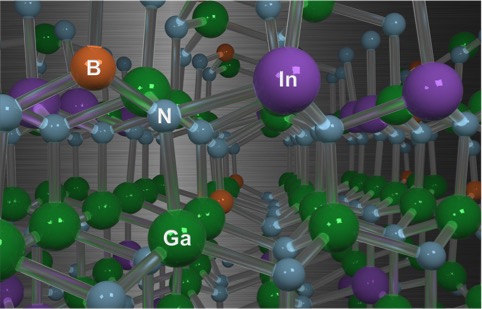
Crystal structure of a BInGaN alloy. Image: Michael Waters and Logan Williams, University of Michigan
High-power white LEDs face the same problem that Michigan Stadium faces on game day — too many people in too small of a space. Of course, there are no people inside of an LED. But there are many electrons that need to avoid each other and minimize their collisions to keep the LED efficiency high. Using predictive atomistic calculations and high-performance supercomputers at the National Energy Research Scientific Computing Center (NERSC), researchers Logan Williams and Emmanouil Kioupakis at the University of Michigan found that incorporating the element boron into the widely used InGaN (indium-gallium nitride) material can keep electrons from becoming too crowded in LEDs, making the material more efficient at producing light. Their work was published this month in Applied Physics Letters.
"For the calculations we used VASP (The Vienna Ab initio simulation package) and approximately 100,000 service units at NERSC," Kioupakis said. "Although these calculations may not be the kind that push the limits of NERSC machines, the reliable computing resources dedicated to energy research at NERSC have been instrumental to our research."
Modern LEDs are made of layers of different semiconductor materials grown on top of one another. The simplest LED has three such layers. One layer is made with extra electrons put into the material. Another layer is made with too few electrons; the empty spaces where electrons would be are called holes. Then there is a thin middle layer sandwiched between the other two that determines what wavelength of light is emitted by the LED. When an electrical current is applied, the electrons and holes move into the middle layer where they can combine together to produce light. But if too many electrons get squeezed in the middle layer to increase the amount of light coming out of the LED, then they may collide with each other rather than combine with holes to produce light. These collisions convert the electron energy to heat in a process called Auger recombination and lower the efficiency of the LED.
A way around this problem is to make more room in the middle layer for electrons (and holes) to move around. A thicker layer spreads out the electrons over a wider space, making it easier for them to avoid each other and reduce the energy lost to their collisions. But making this middle LED layer thicker isn’t as simple as it sounds.
Because LED semiconductor materials are crystals, the atoms that make them up must be arranged in specific regular distances apart from each other. That regular spacing of atoms in crystals is called the lattice parameter. When crystalline materials are grown in layers on top of one another, their lattice parameters must be similar so that the regular arrangements of atoms match where the materials are joined. Otherwise the material gets deformed to match the layer underneath it. Small deformations aren’t a problem, but if the top material is grown too thick and the deformation becomes too strong then atoms become misaligned so much that they reduce the LED efficiency. The most popular materials for blue and white LEDs today are InGaN surrounded by layers of GaN. Unfortunately, the lattice parameter of InGaN does not match GaN. This makes growing thicker InGaN layers to reduce electron collisions challenging.
Williams and Kioupakis found that by including boron in this middle InGaN layer, its lattice parameter becomes much more similar to GaN, even becoming exactly the same for some concentrations of boron. In addition, even though an entirely new element is included in the material, the wavelength of light emitted by the BInGaN material is very close to that of InGaN and can be tuned to different colors throughout the visible spectrum. This makes BInGaN suitable to be grown in thicker layers, reducing electron collisions and increasing the efficiency of the visible LEDs.
Although this material is promising to produce more efficient LEDs, it is important that it can be realized in the laboratory. Williams and Kioupakis have also shown that BInGaN could be grown on GaN using the existing growth techniques for InGaN, allowing quick testing and use of this material for LEDs. Still, the primary challenge of applying this work will be to fine tune how best to get boron incorporated into InGaN at sufficiently high amounts. But this research provides an exciting avenue for experimentalists to explore making new LEDs that are powerful, efficient, and affordable at the same time.
This work was supported by the Designing Materials to 282 Revolutionize and Engineer our Future (DMREF) Program under Award No. 1534221, funded by the National Science Foundation. This research used resources of the National Energy Research Scientific Computing Center, a DOE Office of Science User Facility supported under Contract No. DE-AC02-05CH11231.
About NERSC and Berkeley Lab
The National Energy Research Scientific Computing Center (NERSC) is a U.S. Department of Energy Office of Science User Facility that serves as the primary high performance computing center for scientific research sponsored by the Office of Science. Located at Lawrence Berkeley National Laboratory, NERSC serves almost 10,000 scientists at national laboratories and universities researching a wide range of problems in climate, fusion energy, materials science, physics, chemistry, computational biology, and other disciplines. Berkeley Lab is a DOE national laboratory located in Berkeley, California. It conducts unclassified scientific research and is managed by the University of California for the U.S. Department of Energy. »Learn more about computing sciences at Berkeley Lab.