


2D 'Flat' Boron Yields a Superconducting Surprise
Simulations Run at NERSC Help Reveal Material’s Superconducting Superpowers
April 22, 2016
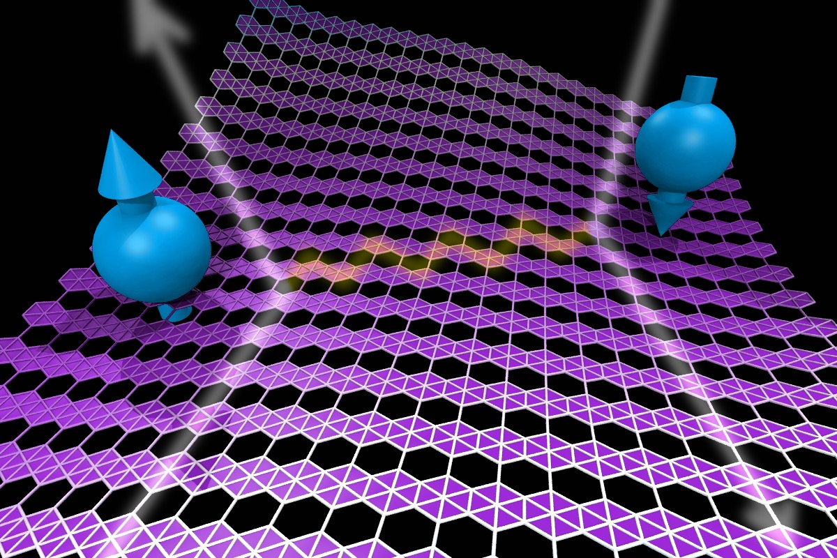
Electrons with opposite momenta and spins pair up via lattice vibrations at low temperatures in 2D boron and give it superconducting properties. Image: Evgeni Penev, Rice University
Density functional theory simulations run at NERSC helped Rice University researchers determine that two-dimensional boron is a natural low-temperature superconductor. In fact, it may be the only 2D material with such potential.
Rice theoretical physicist Boris Yakobson and his co-workers published their calculations, which show that atomically flat boron is metallic and will transmit electrons with no resistance, last month in Nano Letters. The hitch is that it loses its resistivity only when very cold, in this case between 10 and 20 kelvins (roughly, minus-430 degrees Fahrenheit). But for making very small superconducting circuits, it might be the only game in town.
The basic phenomenon of superconductivity has been known for more than 100 years, said Evgeni Penev, a research scientist in the Yakobson group, but had not been tested for its presence in atomically flat boron.
"It's well-known that the material is pretty light because the atomic mass is small," Penev said. "If it's metallic too, these are two major prerequisites for superconductivity. That means at low temperatures, electrons can pair up in a kind of dance in the crystal."
"Lower dimensionality is also helpful," Yakobson said. "It may be the only, or one of very few, two-dimensional metals."
Electrons with opposite momenta and spins effectively become Cooper pairs; they attract each other at low temperatures with the help of lattice vibrations, the so-called "phonons," and give the material its superconducting properties, according to Penev. "Superconductivity becomes a manifestation of the macroscopic wave function that describes the whole sample. It's an amazing phenomenon," he said.
It wasn't entirely by chance that the first theoretical paper establishing conductivity in a 2D material appeared at roughly the same time the first samples of the material were made by laboratories in the United States and China. In fact, an earlier paper by the Yakobson group had offered a road map for doing so.
That 2D boron has now been produced is a good thing, according to Yakobson and lead authors Penev and Alex Kutana, a postdoctoral researcher at Rice. "We've been working to characterize boron for years, from cage clusters to nanotubes to planer sheets, but the fact that these papers appeared so close together means these labs can now test our theories," Yakobson said. "In principle, this work could have been done three years ago as well. "So why didn't we? Because the material remained hypothetical; okay, theoretically possible, but we didn't have a good reason to carry it too far.”
Boron atoms can make more than one pattern when coming together as a 2D material, another characteristic predicted by Yakobson and his team that has now come to fruition. These patterns, known as polymorphs, may allow researchers to tune the material's conductivity "just by picking a selective arrangement of the hexagonal holes," Penev said.
Without the availability of a block of time on several large government supercomputers, including NERSC’s Edison system and resources at the U.S. Army Engineer Research and Development Supercomputing Resource Center, the study would have taken much longer, Yakobson noted.
“The ultimate goal of our research is to develop, simulate and predict new boron nanostructures with desired properties,” he and his colleagues wrote in their latest allocation request to NERSC. To achieve this requires several theoretical methods based on a variety of concepts, ranging from the most accurate ab initio first principles methods suited for small or medium sized systems to tight-binding approximation methods for larger systems. “These theoretical methods are reliable tools to predict, analyze and optimize nanostructure materials, for which we need extensive computational facilities such as the one provided by NERSC.”
NERSC is a Department of Energy Office of Science user facility.
This article was adapted from materials provided by Rice University.
About NERSC and Berkeley Lab
The National Energy Research Scientific Computing Center (NERSC) is a U.S. Department of Energy Office of Science User Facility that serves as the primary high performance computing center for scientific research sponsored by the Office of Science. Located at Lawrence Berkeley National Laboratory, NERSC serves almost 10,000 scientists at national laboratories and universities researching a wide range of problems in climate, fusion energy, materials science, physics, chemistry, computational biology, and other disciplines. Berkeley Lab is a DOE national laboratory located in Berkeley, California. It conducts unclassified scientific research and is managed by the University of California for the U.S. Department of Energy. »Learn more about computing sciences at Berkeley Lab.