


A Roadmap for Engineering Piezoelectricity in Graphene
Doping this ‘Miracle Material’ May Lead to New Array of Nanoscale Devices, Simulations Reveal
February 23, 2012
Linda Vu, lvu@lbl.gov, +1 510 495 2402
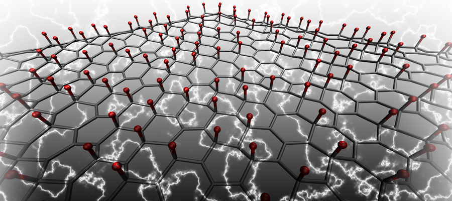
This illustration shows lithium atoms (red) doped on graphene (black hexagons) and generating electricity. Graphic courtesy of Mitchell Ong, Stanford University.
Some scientists refer to graphene as the “miracle material” of the 21st century. Composed of a single sheet of carbon atoms, this material is tougher than diamond, more conductive than copper, and has potential applications in a variety of technologies.
Now with the help of supercomputers at the Department of Energy’s National Energy Research Scientific Computing Center (NERSC), researchers at Stanford University have uncovered yet another hidden talent—with a little chemical doping, graphene can also be transformed into a controllable piezoelectric material. This “engineered piezoelectricity” could lead to new devices like nanoscale chemical and acoustic sensors.
“Our results revealed for the first time a designer piezoelectric phenomenon, unique to the nanoscale, which could bring dynamical control to nanoscale electromechanical devices,” says Mitchell Ong, a postdoctoral researcher at Stanford University.
Ong and Stanford University Professor Evan Reed co-authored a paper about the phenomenon in a recently published issue of ACS Nano.
A Difference in Physics: 2D vs. 3D
From ultrasound scanners to microphones and inkjet printers, many of today’s technologies rely on the piezoelectric effect, also known as “pressure electricity.” Under normal circumstances, piezoelectric materials are electrically neutral: A positive charge in one place cancels out a negative charge nearby. But under pressure, the crystals that make up these materials deform, upsetting the spatial balance of positive and negative and producing a voltage. Part of what makes piezoelectric materials so useful is that the effect can also be reversed—applying an electric field to a crystal will cause it to change shape or deform.
According to Reed, one of the biggest challenges to building electronics with graphene is figuring out how to dynamically control its electronic properties. He notes that because graphene is two-dimensional (2D), the physics that governs it are quite different than that of the three-dimensional (3D) materials used in today’s electronics.
“We’ve had decades to perfect strategies for dynamically controlling electronic properties of bulk [3D] materials, but there are likely radically new methods for 2D graphene, which was discovered relatively recently,” says Reed. “To solve this problem, we had to think outside of the box.”
Making Graphene What it’s Not: Piezoelectric
According to Ong, the team’s out-of –the-box solution was to use the piezoelectric effect to control graphene’s strain and electric properties. There was, however, one little problem: The piezoelectric effect typically only occurs in materials that are inherently piezoelectric, and graphene is not.
Using NERSC’s Franklin and Carver supercomputers, Ong and Reed ran calculations to see if they could engineer piezoelectric properties into graphene by chemically doping it with hydrogen (H), fluorine (F), potassium (K) or lithium (Li) atoms on one side of the material.
“Our results revealed that chemical doping can in fact induce piezoelectricity in 2D graphene of magnitudes comparable to known 3D materials,” says Ong. “Unlike existing piezoelectric materials, this fundamentally new form of engineered piezoelectricity is made possible by the 2D nanoscale nature of graphene.”
“The strain or deformation generated in piezoelectric materials is proportional to the magnitude of the electric field applied, so this phenomenon would allow us to dynamically control the electronic properties of graphene,” says Ong.
Ong notes that previous experiments have shown that adsorbates can be spatially patterned on the surface of graphene, which has led the researchers to the idea of engineering devices by inducing piezoelectricity selectively. “This experimental work, combined with our results, hints that devices could be created where strains are spatially concentrated to control local electrical and chemical properties,” says Ong.
The team hopes that this work could potentially lead to new piezoelectric devices based not just on graphene, but other 2D and low-dimensional materials as well. Armed with their NERSC results, Ong and Reed plan on testing these simulations in laboratory experiments.
“NERSC resources made it possible to do this work,” says Ong. “These resources allowed us to scale up and study very large system sizes, which would have been difficult to do on our local cluster.”
Their work is partially supported by the Department of Energy’s Office of Basic Energy Sciences in the Office of Science.
About NERSC and Berkeley Lab
The National Energy Research Scientific Computing Center (NERSC) is a U.S. Department of Energy Office of Science User Facility that serves as the primary high performance computing center for scientific research sponsored by the Office of Science. Located at Lawrence Berkeley National Laboratory, NERSC serves almost 10,000 scientists at national laboratories and universities researching a wide range of problems in climate, fusion energy, materials science, physics, chemistry, computational biology, and other disciplines. Berkeley Lab is a DOE national laboratory located in Berkeley, California. It conducts unclassified scientific research and is managed by the University of California for the U.S. Department of Energy. »Learn more about computing sciences at Berkeley Lab.